condition 1: ANALOG
MSB | 0 | 0 | G2 | G1 | G0 | O2 | O1 | O0 | SEL7 | SEL6 | SEL5 | SEL4 | SEL3 | SEL2 | SEL1 | SEL0 | LS |
Selects analog mux input at address SEL7-SEL0 (256 possible analog inputs), with ADC gain of G2-G0 (8 gains), with ADC offset of O2-O0 (8 offsets). On versions above 1 Mega BPS, programmable gain and offset is not available at this time. For more then 256 analog inputs, gain or offset bits must be sacrificed.
condition 2: DIGITAL
* means don't care
*
MSB | 0 | 1 | X | X | X | X | X | X | SEL7 | SEL6 | SEL5 | SEL4 | SEL3 | SEL2 | SEL1 | SEL0 | LSB |
Selects digital mux input at address SEL7-SEL0 (256 possible digital
mux inputs). The digital mux supplies serial data of 1 word length for
each input. Standard with each encoder are the following digital mux inputs:
DIGITAL MUX INPUT | SEL7-SEL0 | |
|
||
BILEVEL WORD 1 | 250 | |
BILEVEL WORD 2 | 251 | |
**BILEVEL WORD 3 | 248 | **OPTION |
**BILEVEL WORD 4 | 249 | **OPTION |
**BILEVEL WORD 5 | 254 | **OPTION |
**BILEVEL WORD 6 | 255 | **OPTION |
SERIAL SYNCHRONOUS WORD | 252 | |
RS232/RS422 ASYNCHRONOUS WORD | 253 | |
FRAME COUNTER | 240 | |
IRIG TIME B | 241 |
condition 3: SYNC
* X means don't care
*
MSB | 1 | 0 | X | X | SY11 | SY10 | SY9 | SY8 | SY7 | SY6 | SY5 | SY4 | SY3 | SY2 | SY1 | SY0 | LSB |
Causes sync data SY11-SY0 to be inserted into the PCM data stream. For word sizes less than 12 bits, the syncs LSB's are discarded.
condition 4: SYNC AND RESET FRAME
* X means don't care
*
MSB | 1 | 1 | X | X | SY11 | SY10 | SY9 | SY8 | SY7 | SY6 | SY5 | SY4 | SY3 | SY2 | SY1 | SY0 | LSB |
Causes sync data SY11-SY0 to be inserted into the PCM data stream and the EEPROM address counter to reset. Resetting the counter causes the completion of one complete PCM major frame. For word sizes less than 12 bits, the syncs LSB's are discarded.
The 4 conditions described above can be used to generate any possible frame with sub and super commutation up to a major frame length of 2048.
PC software is provided with the encoder, which performs the programming. When executing the software and the main programming menu is displayed on the PC, RTS is false so the encoder acts as if the PC is not connected. RTS is set true only after a command is issued.
One of the commands provided with the PC software is installation. This command needs to be executed only once to determine which COM port the encoder is connected to. The COM port information is stored on disk..
The encoder EEPROM is programmed from files stored on your PC disk. These files can be generated with the software provided or can be manually generated or edited. The file format is now described. Each line (record) in the file contains one byte (8 bits) of information. Each two consecutive bytes form one word of EEPROM data. The most significant byte is stored first.
For example:
BYTE# | VALUE | MEANING |
|
||
1 | $40 | most significant byte stored at EEPROM address 0 |
2 | 253 | least significant byte stored at EEPROM address 0 |
3 | 58 | most significant byte stored at EEPROM address 1 |
4 | 3 | least significant byte stored at EEPROM address 1 |
5 | $CA | most significant byte stored at EEPROM address 2 |
6 | $AA | least significant byte stored at EEPROM address 2 |
After programming, page 1 of the EEPROM will look as follows:
adrs 0 MSB -> 0 1 0 0 0 0 0 0 1 1 1 1 1 1 0 1 <- LSB
adrs 1 MSB -> 0 0 1 1 1 0 1 0 0 0 0 0 0 0 1 1 <- LSB
adrs 2 MSB -> 1 1 1 0 1 0 1 0 1 0 1 0 1 0 1 0 <- LSB
This program will generate a PCM frame length of 3 words. The first
word will be RS232/RS422 data. The second word will be analog channel at
mux address 3, of gain given by code 7 and offset given by code 2. The
third word will be a sync word of alternating ones and zeroes.
A/D Converters:
1MBit Standard | |
1MBit Programmable Gain & Offset | |
10MBit Standard | |
10MBit Programmable Gain & Offset |
The PGA provides 8 gains from one to ten:
STANDARD EEPROM CODE
|
|
|
|
|
|||
|
|
|
|
|
|
|
|
|
|
|
|
|
|
|
|
|
|
|
|
|
|
|
|
|
|
|
|
|
|
|
|
The POA provides 8 offsets from +0.5 Volts to -3.0 Volts:
STANDARD EEPROM CODE
OFFSETS O2 O1 O0
+0.5 Volts 0 0 0
0 Volts 0 0 1
-0.5 Volts 0 1 0
-1.0 Volts 0 1 1
-1.5 Volts 1 0 0
-2.0 Volts 1 0 1
-2.5 Volts 1 1 0
-3.0 Volts 1 1 1
Consult factory for non-standard gains and offsets. Gain and offset is programmed on a PCM word sample basis. Shown below is a block diagram of the PGA, POA and ADC:
Note that offset is inserted after gain. Gain and offset should be selected
to condition to ADC full scale (-2.5V to +2.5V).
Example:
The input from the Analog Multiplexer ranges from 0 to 5 volts. Select
a gain of 1 and an offset of -2.5 volts.
Example:
The input from the Analog Multiplexer ranges from 0 to 0.5 volts. Select
a gain of 10 and an offset of -2.5 volts.
Example:
The input from the Analog Multiplexer ranges from -0.25 to +0.25 volts.
Select a gain of 10 and an offset of 0.0 volts.
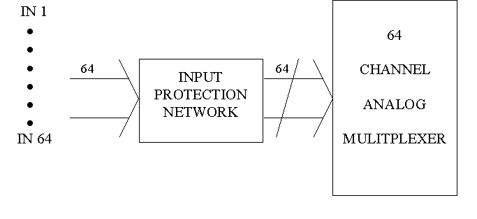
Various signal conditioning/multiplexing hybrids are available for the PCM Encoder. These hybrids are integrated within the encoder and are described in this section.
Input Amplitude: 0.1 volts to 10 volts peak to peak without adjustment.
Input Impedance: 100k ohms minimum.
Internal Oscillator: 0 to +50°C, + or -5ppm, aging 10-7/day (optional).
Power: +24 to 32 VDC.
IRIG B Timing Configuration
The IRIG timing has form hours through microseconds as shown below:
The IRIG data takes 4, 16 bit words and is in the following format:
Bit Bit Bit Bit Bit Bit Bit Bit Bit Bit Bit Bit Bit Bit Bit Bit
63 62 61 60 59 58 57 56 55 54 53 52 51 50 49 48
X X X X X X 200 100 80 40 20 10 8 4 2 1
| | Days |
Bit Bit Bit Bit Bit Bit Bit Bit Bit Bit Bit Bit Bit Bit Bit Bit
47 46 45 44 43 42 41 40 39 38 37 36 35 34 33 32
X X 20 10 8 4 2 1 X 40 20 10 8 4 2 1
| | Hours | | Minutes |
Bit Bit Bit Bit Bit Bit Bit Bit Bit Bit Bit Bit Bit Bit Bit Bit
31 30 29 28 27 26 25 24 23 22 21 20 19 18 17 16
X 40 20 10 8 4 2 1 800 400 200 100 80 40 20 10
| | Seconds | Milliseconds |
Bit Bit Bit Bit Bit Bit Bit Bit Bit Bit Bit Bit Bit Bit Bit Bit
15 14 13 12 11 10 9 8 7 6 5 4 3 2 1 0
8 4 2 1 800 400 200 100 80 40 20 10 8 4 2 1
| Milliseconds | Microseconds |
Programming the encoder to select the IRIG Time word places the IRIG time word into the PCM bit stream. Multiple words are programmed to obtain all 64 Bits. The least significant bit of the 64 bit IRIG time word is transmitted first.
The EEPROM code (section 1.2) to select one PCM word length of IRIG time is:
EEPROM Upper Byte (Hex) $40
EEPROM Lower Byte (Decimal) 241
The following PCM EEPROM program at 10 bits per word will place 70 bits of IRIG time data into the PCM data stream:
$40, 241 LSB Transmitted First
$40, 241
$40, 241
$40, 241
$40, 241
$40, 241
$40, 241 Most Significant Upper Bits are Zero Filled
The following PCM EEPROM program at 10 Bits/word will place 20 bits of IRIG Time data into the PCM data stream:
$40, 241 LSB
$40, 241
The frame counter length is dependent on the number of bits per word:
Bits/Word | Frame Counter Length |
|
|
6 | 24 |
7 | 21 |
8 | 24 |
9 | 27 |
10 | 20 |
11 | 22 |
12 | 24 |
Programming the encoder to select the frame counter (for the digital mux) always reads the most significant word of frame count first. Multiple reads complete the total number of words.
The EEPROM code (section 1.2) to select one PCM word length of frame count is:
EEPROM Upper Byte (Hex) $40
EEPROM Lower Byte (Decimal) 240
The following PCM EEPROM program at 8 bits/word will place 24 bits of frame count into the PCM data stream:
$40, 240
$40, 240
$40, 240 Least Significant Frame Counter Bits
0 DEGCLK: Pin 2, Clock output at bit rate. Eight bit rates are provided.
The bit rate selection is stored in internal EEPROM and is initialized
at power up and after programming.
STANDARD BIT RATES | |
1 MEGA BIT VERSION | 10 MEGA BIT VERSION |
|
|
1MBIT | 10MBIT |
500KBIT | 5MBIT |
250KBIT | 2.5MBIT |
125KBIT | 1.25MBIT |
62.5KBIT | 625KBIT |
31.25KBIT | 312.5KBIT |
15.625KBIT | 156.25KBIT |
7.8125KBIT | 78.125KBIT |
Note: Non-standard internally generated bit rates are a factory option. Eight bit rates are provided in a divide by 2 fashion.
Note: An external clock source can generate non-standard desired bit rates. Bit rates for both encoder versions can go down to DC.
CODE: Pin 3, one of nine PCM output codes. The output code selection is stored in internal EEPROM and is initialized at power up and after programming. The output code signal is output to the external premod filter connector for pre-modulation filtering. The filtered signal is output is available at the external premod filter.
POSSIBLE OUTPUT CODES
NRZ-L
NRZ-M
NRZ-S
BIO-L
BIO-M
BIO-S
DM-M
DM-S
RNRZ-L
232PLS: Pin 4, pulse output. This pulse occurs each time an asynchronous word (RS232 or RS422) is inserted into the PCM data stream. This signal can be sued to monitor the asynchronous data word inserted.
DGND: Pin 6, Digital ground. Reference bilevel inputs, PCM outputs, clocks, diagnostic signals to this ground.
BI0, BI1, ... BI10, BI11: Pins 7 to 18, Bilevel inputs, word 1.
BI0 -> LSB.
BI11 -> MSB.
LSB's are discarded for word sizes less than 12.
BI12, BI13, ... BI22, BI23: Pins 22 to 33, Bilevel inputs, word 2.
BI12 -> LSB.
BI23 -> MSB.
LSB's are discarded for word sizes less than 12.
RTS: Pin 19, Request to Send, for encoder programming. Connect to PC COM1 or COM2 port for programming. Referenced to DGND or B+RTN.
T232: Pin 20, Transmit RS232 asynchronous serial data output from encoder to PC during encoder programming. Connect to PC COM1 or COM2 port for programming. Referenced to DGND or B+RTN.
R232: Pin 21, Receive RS232 asynchronous serial data input to encoder from PC for programming encoder. Connect to PC COM1 or COM2 port for programming. Referenced to DGND or B+RTN.
DGND: Pin 34, Digital ground. Reference bilevel inputs, PCM outputs, clocks, diagnostic signals to this ground. Connected to AGND and B+RTN internal to the encoder.
B+RTN: Pin 38, B+ return (Encoder power ground).
B+RTN: Pin 39, B+ return (Encoder power ground).
B+28V: Pin 40, B+ (+28V +- 6V).
B+28V: Pin 41, B+ (+28V +- 6V).
CHASSIS GND: PIN 42, Case ground, isolated from all other grounds.
R422+: Pin 43, RS422 asynchronous receive data input, positive polarity
referenced to R422-.
J1 51 PIN CONFIGURATION
R422-: Pin 44, RS422 receive asynchronous data input, negative polarity referenced to R422+ when the asynchronous data port is programmed for RS422 specification. If the asynchronous data port is programmed for RS232 specification, this pin is the positive polarity RS232 asynchronous data input referenced to DGND or B+RTN. The asynchronous data port specification selection is stored in internal EEPROM and is initialized at power up and after programming (RS232 or RS422).
FRMSNC: Pin 48, Frame sync pulse output.
WRDSNC: Pin 49, Word sync pulse output.
2X CLKIN: Pin 50, Clock input, two times the bit rate. Connect to 2X CLKOUT for internally generated bit rates. For externally generated bit rates, connect to an external clock source of the desired bit rate (CMOS or TTL).
2X CLKOUT: Pin 51, Clock output, two times the bit rate. Connect to 2X CLKIN for internally generated bit rates.
0 DEGCLK: Pin 2, Clock output at bit rate. Eight bit rates are provided. The bit rate selection is stored in internal EEPROM and is initialized at power up and after programming.
STANDARD BIT RATES
1 MEGA BIT VERSION 10 MEGA BIT VERSION
1MBIT 10MBIT
500KBIT 5MBIT
250KBIT 2.5MBIT
125KBIT 1.25MBIT
62.5KBIT 625KBIT
31.25KBIT 312.5KBIT
15.625KBIT 156.25KBIT
7.8125KBIT 78.125KBIT
Note: Non standard internally generated bit rates are a factory option. Eight bit rates are provided in a divide by 2 fashion.
Note: An external clock source can generate non standard desired bit rates. Bit rates for both encoder versions can go down to DC.
CODE: Pin 3, One of seven PCM output codes. The output code selection is stored in internal EEPROM and is initialized at power up and after programming. The output code signal is output to the external premod filter connector for pre-modulation filtering. The filtered signal is output is available at the external premod filter.
POSSIBLE OUTPUT CODES
NRZ-L
NRZ-M
NRZ-S
BIO-L
BIO-M
BIO-S
RNRZ-L
232PLS: Pin 68, Pulse output. This pulse occurs each time an asynchronous word (RS232 or RS422) is inserted into the PCM data stream. This signal can be used to monitor the asynchronous data word inserted.
DGND: Pin 52, 53, 66, 67 Digital ground. Reference bilevel inputs, PCM outputs, clocks, diagnostic signals to this ground. Connected to AGND and B+RTN internal to the encoder.
BI0, BI1,...BI10, BI11: Pins 26 down to 15, Bilevel inputs, word 1
BI0 -> LSB.
BI11 -> MSB.
LSB's are discarded for word sizes less than 12.
BI12, BI13,...BI22, BI23: Pins 51 down to 40, Bilevel inputs, word 2
BI12 -> LSB.
BI23 -> MSB.
LSB's are discarded for word sizes less than 12.
BI24, BI25,...BI34, BI35: Pins 39 down to 28, Bilevel inputs, word 3
BI24 -> LSB
BI35 -> MSB
LSB's are discarded for word sizes less than 12.
BI36, BI37,...BI46, BI47: Pin 27, Pins 14 down to 4. Bilevel inputs, word 4
BI36 ->LSB.
BI47 ->MSB.
LBS's are discarded for word sizes less than 12.
BI48, BI49,...BI58, BI59: Pins 65 down to 54, Bilevel inputs, word 5
BI 48 -> LSB.
BI 59 -> MSB.
LBS's are discarded for word sizes less than 12.
BI60, BI61,...BI70, BI71: Pins 92 down to 81, Bilevel inputs, word 6
BI 60 -> LSB.
BI 71 -> MSB.
LBS's are discarded for word sizes less than 12.
RTS: Pin 96, Request to Send, for encoder programming. Connect to PC COM1 or COM2 port for programming. Referenced to DGND or B+RTN.
J1 100 PIN CONFIGURATION
T232: Pin 98, Transmit RS232 asynchronous serial data output from encoder to PC during encoder programming. Connect to PC COM1 or COM2 port for programming. Referenced to DGND or B+RTN.
R232: Pin 97, Receive RS232 asynchronous serial data input to encoder from PC for programming encoder. Connect to PC COM1 or COM2 port for programming. Referenced to DGND or B+RTN.
B+RTN: Pin 77, B+ return (Encoder power ground).
B+RTN: Pin 78, B+ return (Encoder power ground).
B+28V: Pin 79, B+ (+28V +- 6V).
B+28V: Pin 80, B+ (+28V +- 6V).
CHASSIS GND: PIN 76, Case ground, isolated from all other grounds.
R422+: Pin 94, RS422 asynchronous receive data input, positive polarity referenced to R422-.
R422-: Pin 95, RS422 receive asynchronous data input, negative polarity referenced to R422+ when the asynchronous data port is programmed for RS422 specification. If the asynchronous data port is programmed for RS232 specification, this pin is the positive polarity RS232 asynchronous data input referenced to DGND or B+RTN. The asynchronous data port specification selection is stored in internal EEPROM and is initialized at power up and after programming (RS232 or RS422).
FRMSNC: Pin 100, Frame sync pulse output.
WRDSNC: Pin 99, Word sync pulse output.
2X CLKIN: Pin 75, 2X Clock input. Connect to 2X CLKOUT for internally generated bit rates. For externally generated bit rates, connect to an external clock source of the desired bit rate (CMOS or TTL) times 2.
2X CLKOUT: Pin 74, 2X Clock output. Connect to 2X CLKIN for internally
generated bit rates.
J1 100 PIN CONFIGURATION
Some update possibilities are time code (PCM digital word) generation,
both 8 and 9 bit asynchronous data format, user specified asynchronous
and synchronous data format, expanded DVM mode, etc.
PROG9.EXE - Execute this program to program the encoder.
PFIG.DAT - Encoder configuration file that must be located in the same directory as PROG9.EXE.
PINST.DAT - PC installation file that must be located in the same directory as PROG9.EXE.
USER.DOC - File containing this document.
COM PORT PIN:
ENCODER SIGNAL (25 pin style)
RTS - Request To Send, J1-19 4
T232 - Serial Data from Encoder to PC, J1-20 3
R232 - Serial Data from Encoder to PC, J1-20 2
The encoder must be powered up.
The encoder must be powered up
The encoder must be powered up.
PCM WORD FORMAT FOR RS422 OR RS232 ASYNCHRONOUS DATA
With BIT 11 the most significant bit and BIT 0 the least significant bit:
BIT 11 to BIT 4: Data.
BIT 3: Set to 1 if FIFO buffer underflowed (no new data to transmit), set to zero otherwise. When this bit is set to 1, the data transmitted in BIT 11 to BIT 4 is repeated from the previous asynchronous data.
BIT 2: Set to 1 if FIFO buffer overflowed, set to zero otherwise. When this bit is set to 1, the data transmitted in BIT 11 to BIT 4 is the most recent received data.
BIT 1: Parity.
BIT 0: Spare.
Note: As the number of bits per word is reduced from 12, the least significant bits are discarded (not transmitted).
Note: Both 8 and 9 bit asynchronous data formats can be ordered, see boot mode.
RS422/RS232 ASYNCHRONOUS DATA BAUD RATES
0 125.00K BAUD 16 31.250K BAUD
1 62.50K BAUD 17 15.625K BAUD
2 31.25K BAUD 18 7812.5 BAUD
3 15.625K BAUD 19 3906 BAUD
4 7812.5 BAUD 20 1953 BAUD
5 3906 BAUD 21 977 BAUD
6 1953 BAUD 22 488 BAUD
7 977 BAUD 23 244 BAUD
8 41.666K BAUD 24 9600 BAUD
9 20.833K BAUD 25 4800 BAUD
10 10.417K BAUD 26 2400 BAUD
11 5208 BAUD 27 1200 BAUD
12 2604 BAUD 28 600 BAUD
13 1302 BAUD 29 300 BAUD
14 651 BAUD 30 150 BAUD
15 326 BAUD 31 75 BAUD
Note: Other baud rates are optionally specified when ordered
The Clear To Send (CTS) signals (both RS422 and RS232) are set true by the encoder when the FIFO buffer is not full. CTS can be polled by external hardware to prevent FIFO buffer overflow when transmitting asynchronous data to the encoder. CTS can be programmed to be set false when less then a certain number of FIFO locations are empty and set true otherwise. The CTS time parameter is stored in EEPROM and is initialized at power up and after programming. This parameter in useful when the external hardware buffers its data link to the encoder.
The encoder outputs the diagnostic signal 232PLS, which is a pulse that
occurs when an asynchronous data word is inserted into the PCM data stream.
This signal can be used to monitor the asynchronous data word inserted.
The encoder also outputs the 8 bit data byte on its RS232 programming port
at the programmed baud rate when the data and status is inserted into the
PCM data stream.
If not using an external clock, connect 2X CLOCKIN to 2X CLOCKOUT.
Connect to PC if programming.
Apply power.
2. Connectors J2, J3 and J4 contain precision analog signals and J1 contains digital signals with fast rise times. To avoid noise pickup J1 signals should be separated from J1, J2, J3 and J4 signals. Clock signals are good noise sources and these lines should be kept as short as possible. The loop from clockout to clockin should be kept as short as possible (Close to the connector). Wires not allocated on the connector pinout should be cut off at the mating connector.
3. Power ground (J1-38, J1-39) pins should both be connected to the power supply return. Power ground and B+ lines should be as low resistance as possible.
4. Analog differential plus and minus input signals on multiplexer connectors should be run as twisted pairs. Analog ground may be used as a shield. This applies to differential signals only.
5. Analog ground signals should all be connected to the transducer ground
source to provide as low resistance as possible.
Back to PCM | Back To PCM2 |